Copyright © 2019 深圳市蓝星宇电子科技有限公司 All Rights Reserved 粤ICP备12009628号 | 友情链接(旧版网站)


|
ASML Twinscan XT 400L
咨询购买
|
ASML Twinscan XT 400L
.png)
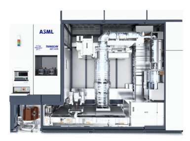
TWINSCAN XT:400L
The TWINSCAN XT:400L is ASML’s latest-generation i-line lithography system, using a mercury vapor lamp to print features down to 220 nm
Key features & benefits
In addition to increased productivity, the XT:400L introduces new options to assist advanced applications with high topography (such as 3D-NAND) and small CD and CDU (such as critical layers in Logic or analog applications).
Just like previous models, the XT:400L is a dual-stage lithography system designed for volume production of 200 mm and 300 mm wafers down to a 220 nm resolution.
High throughput and yield are combined with fast reticle exchange times and lot streaming to provide the lowest cost of operation.
The TWINSCAN XT:400L is able to achieve a throughput of ≥ 230 300 mm wafers per hour (≥ 220 using the high-resolution option), and ≥ 250 200 mm wafers per hour. Thanks to a bridge tool, customers are able to convert between 200 mm and 300 mm wafers with less than a week of machine downtime.
The TWINSCAN XT:400L contains a variable 0.65 NA 365 nm projection lens with an advanced lens manipulator and imaging enhancement options. Customers can achieve a production resolution of 350 nm (standard), 280 nm (annular illumination), or 220 nm (annular illumination plus high-resolution option).
Using TOP-2, the XT:400 is able to achieve an improved overlay of ≤ 20 nm for advanced applications such as 3D-NAND staircase exposures. An extended leveling range allows better on-product overlay and focus performance, even for large topology situations.
The SMASH Sensor enables more robust mark integration when using opaque hard masks, using two additional alignment wavelengths (near- and far-infrared as well as red and green).
The level sensor, in combination with the TWINSCAN leveling approach, virtually eliminates differences between inner die and edge die and ensures high yield across the entire 300 mm wafer. Customers can achieve a production resolution of 350 nm (standard), 280 nm (annular illumination), or 220 nm (annular illumination plus high-resolution option).
Copyright © 2019 深圳市蓝星宇电子科技有限公司 All Rights Reserved 粤ICP备12009628号 | 友情链接(旧版网站)
咨询电话
廖经理 13538131258

